|
|
|||||
| intern | ||||||
|
|
||||||
| ||||||||||
InP membrane on silicon devices for all-optical signal processingResearch Area: Heterogeneous integration technology for silicon photonics , Silicon photonics for telecom, datacom and interconnect Main Researcher: Martijn Tassaert Using heterogeneous integration of III-Vs on silicon-on-insulator, several active devices have already been successfully demonstrated. In these demonstrations, electrical current was used to pump or control the device. To achieve this, the III-V consists of an active region within a diode structure that is electrically contacted. As these electrical contacts need to be far enough from the optical mode to avoid excessive losses, the waveguides used have to be at least 500 nm thick. This limits the confinement that can be achieved in the active region of the device. However, if optical excitation of the semiconductor gain medium were used instead of electrical pumping, it would be possible to dramatically reduce the thickness of the active III–V waveguide, as current injection and ohmic contact layers would no longer be required. As a result, one can leverage the high index contrast between the III–V and the surrounding air and DVS-BCB cladding to create III–V membrane waveguides with a much higher confinement in the active region. This stronger confinement can bring the design advantage of stronger light-matter interactions with lower total power consumption, a very relevant consideration for advanced on-chip optical signal processing. In figure 1, an SEM image and device cross section of a 100 nm thick III-V membrane waveguide is shown. Because of the high index contrast, a confinement factor of more than 18% is achieved in the triple quantum well active region. Using this device, several applications can be achieved. First of all, all-optical gates for use as a packet switching component have been realized. In this case, the device is optimized to have an as low as possible power consumption, with an as high as possible extinction ratio at the cost of slower switching (1-2 ns). An extinction ratio of more than 40 dB has been achieved in a device of only 150 um long, using a pump power of 4.5 dBm. By further optimization of the device fabrication, it is expected that pump power can be further reduced by 5 dB. Using membrane gates as switching elements, also a full 1x4 switch has been demonstrated based on the broadcast-and-select switching architecture. 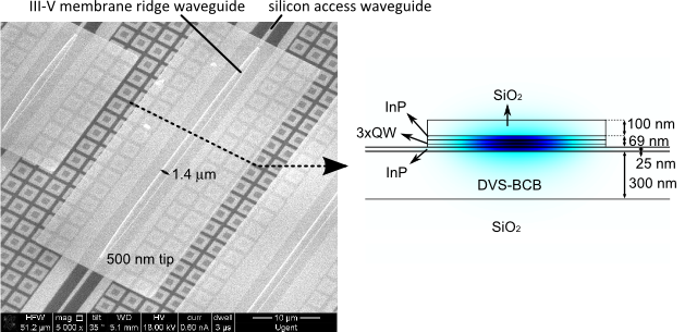
Figure 1: SEM micrograph of fabricated membrane ridge waveguide with plotted mode profile showing the very high confinement of light. Next to this, the membrane gates can also be optimized for high speed signal processing applications. By optimization of the fabrication, the carrier lifetime which limits the device speed can be engineered to the required value. In one application, the membrane gate is used as a saturable absorber. Because of the high confinement factor in the active region, a highly non-linear device transmission is achieved. This can be used to regenerate low extinction ratio input signals (see figure 2). Using a 100 um long device, an extinction ratio improvement from 2 dB to more than 5 dB (up to 6.2 dB at 1530 nm) was achieved over the entire C-band, leading to a receiver sensitivity improvement of more than 3.6 dB (up to 4.5 dB at 1530 nm). 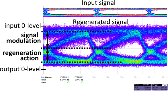
Figure 2: Regeneration action in the membrane waveguide. The additional absorption when the input signal is low increases the extinction ratio of the output signal . Other people involved: Publications |