|
| |
Deposited SOI technology for photonic application Research Area:
Optical signal processing Main Researcher: Shankar Kumar Selvaraja
With ever increasing complexity and density of photonic integrated circuits the need for multilayer functionality is arising for next generation photonic circuitry. Even though mono-crystalline silicon-on-insulator exhibits superior optical quality it is difficult to realize multilayer circuitry based on this material. Deposited Si is a very good candidate for such application, however. The deposited material can be amorphous or polycrystalline depending on the deposition technique and parameters. The two popular deposition processes used in CMOS fabrication process are low-pressure chemical vapor deposition (LPCVD) and Plasma enhanced chemical vapor deposition (PECVD).
We have explored deposited silicon using LPCVD and PECVD techniques in 200mm CMOS deposition tools. LPCVD is used for polycrystalline and PECVD is used amorphous silicon deposition. During amorphous Si deposition the temperature is kept at 300C, which enables us to deposit on variety of substrates (above CMOS, polymers, etc…).
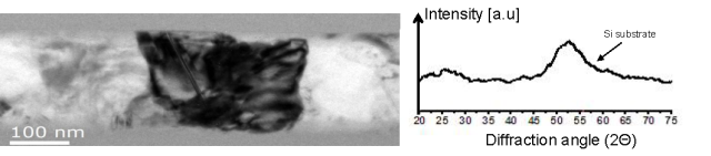
Left- TEM cross-section of polycrystalline Si, Right- XRD on amorphous Si
From our optical characterization, we measure a propagation loss of 3.45dB/cm for a photonic wire of 480nm wide and 220nm thick. We estimate the bulk absorption in amorphous Si to be ~0.7dB/cm
Using our low-loss amorphous silicon we have fabricated two layers of photonic circuit on top of eachother, some times refered as 3D photonic circuit. The two photonic layers were optically coupled through shallow etch gratings as Optical Via's (see figure below). This clearly demonstrates the feasibility of amorphous Si for multilayer photonic circuitry.
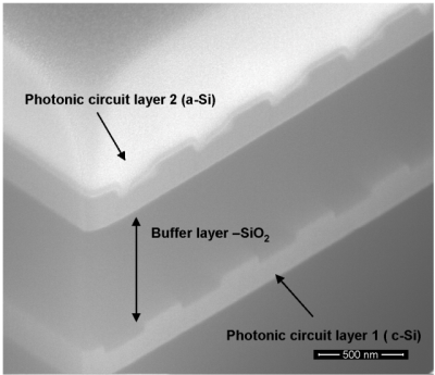
Optical via in Si using shallow etched gratings
Photonic wires (500nmX220nm) fabricated in polycrystalline Si (using LPCVD) measured a propagation loss of 13.4 dB/cm. Though this propagation loss is higher than amorphous silicon, we have identified certain area of application.
Using polycrystalline silicon we have made planar bragg stack on a 200mm silicon wafer, this can be used as high quality cavities.
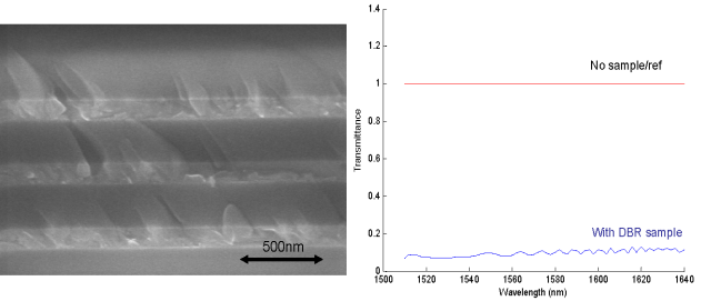
Left- SEM cross-section of a fabricated DBR using poly-Si/SiO2, Right- Measured reflection of a bragg mirror (courtesy prof. S. Unlu, Boston Uni)
PhD thesises PublicationsInternational Journals
-
S. Clemmen, A. Perret, S. Selvaraja, W. Bogaerts, D. Van Thourhout, R. Baets, Ph. Emplit, S. Massar,
Generation of correlated photons in hydrogenated amorphous silicon waveguides, Optics letters, 35(20), p.3483-3485 doi:10.1364/OL.35.003483 (2010)
 . . -
S. Selvaraja, W. Bogaerts, D. Van Thourhout, M. Schaekers,
Thermal trimming and tuning of hydrogenated amorphous silicon nano-photonic devices, Applied Physics Letters, 97 (7), doi:10.1063/1.3479918 (2010) .
-
S. Selvaraja, Erik Sleeckx, Marc Schaekers, W. Bogaerts, D. Van Thourhout, P. Dumon, R. Baets,
Low-Loss Amorphous Silicon-On-Insulator Technology for Photonic Integrated Circuitry, Optics Communications, 282(9), p. 1767-1770 doi:10.1016/j.optcom.2009.01.021 (2009) .
International Conferences
-
A. Omari, H. Shinchi, P. Geiregat, D. Van Thourhout, Z. Hens,
Characterisation of PbS/CdS Qdot absorption on SOI waveguides, Poceedings Symposium IEEE Photonics Society Benelux Chapter, 2012, Mons , Belgium, p.295-298 (2012) .
-
S. Selvaraja, P. Dumon, W. Bogaerts, D. Van Thourhout, R. Baets,
Amorphous silicon: Material for Photonic-Photonic and Electronic-Photonic Integration, 14th Annual Symposium of the IEEE Photonics Benelux Chapter, Belgium, p.137-140 (2009) .
-
S. Selvaraja, D. Vermeulen, Marc Schaekers, Erik Sleeckx, W. Bogaerts, G. Roelkens, P. Dumon, D. Van Thourhout, R. Baets,
Highly Efficient Grating Coupler between Optical Fiber and Silicon Photonic Circuit, Conference on Lasers and Electro-Optics (CLEO) 2009 , United States, p.CTuC6 doi:10.1364/cleo.2009.ctuc6 (2009) .
-
S. Selvaraja, W. Bogaerts, P. Dumon, D. Van Thourhout, R. Baets,
Amorphous silicon photonic crystals made with 193nm lithography, The 8th International Photonic & Electromagnetic Crystal Structures Meeting (PECS), Australia, (2009) .
-
S. Selvaraja, P. Dumon, W. Bogaerts, D. Van Thourhout, R. Baets, E. Sleeckx, M. Schaekers,
Demonstration Of Optical Via And Low-Loss Optical Crossing For Vertical Integration Of Silicon Photonic Circuit, PHOTONICS 2008:The International Conference on Fiber Optics and Photonics (BEST PAPER AWARD), India, (2008) .
-
P.P.P. Debackere, P. Bienstman, R. Baets,
Experimental Characterization of Biosensor based on Surface Plasmon Nano Interferometer, Leos Annual Meeting, United States, p.TuY2 doi:10.1109/leos.2008.4688628 (2008) .
-
S. Selvaraja, D. Van Thourhout, R. Baets,
Fabrication of photonic integrated circuits using high resolution CMOS fabrication process, ePIXnet Springshool 2008, Italy, (2008) .
-
S. Selvaraja, D. Van Thourhout, R. Baets, E. Sleeckx, M. Schaekers,
Deposited silicon-on-insulator material technology for photonic integrated circuitry, 12th IEEE/LEOS Benelux Annual Symposium 2007, Belgium, p.15-18 (2007) .
-
S. Selvaraja, E.Sleeckx, W. Bogaerts, M. Schaekers, P. Dumon, D. Van Thourhout, R. Baets,
Low loss amorphous silicon photonic wire and ring resonator fabricated by CMOS process, 33rd European conference on Optical communication (ECOC) , Germany, p.PD 2.2 (2007) .
-
S. Selvaraja, M.Schaekers, W. Bogaerts, D. Van Thourhout, R. Baets,
Polycrystalline silicon as waveguide material for advanced photonic, 11th IEEE/LEOS Benelux Annual Workshop 2007, Netherlands, (2007) .
National Conferences
-
S. Selvaraja, R. Baets, D. Van Thourhout,
Nanophotonic integrated chip fabricated by CMOS technology, 8th FirW PhD Symposium, Belgium, (2007) .
Back to overview
|